Preparation of new nanostructured Yb/Si alloys
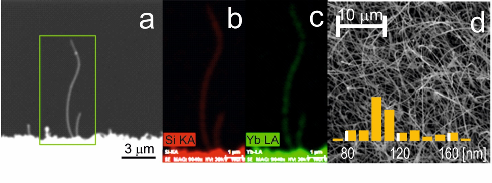 Pulsed laser ablation of a divided Si/Yb target in an oven at temperatures between 800 and 1000 °C was performed for the preparation of nanostructures of ytterbium silicide. The nanostructured deposit was formed by nanowires, nanocolumns, and nanoparticles. The nanoparticles prepared at 800 °C were made of Yb3Si5 alloy, while nanocolumns were face-centered cubic structures together with a monoclinic phase, so far unknown for Yb/Si alloy. At 1000 °C, the prepared nanowires and nanocolumns are amorphous and decorated with nanocrystals with face-centered cubic-structured material. Nanowires prepared at 1000 °C are semiconductive at room temperature with a conductivity of 132.9 W.cm, comparable to highly doped silicon. Characterization of new structures is ongoing at ICPF and other institutes of CAS.