Deposition of thin layers by laser ablation technique
The Group is focused on a long-term basis on the deposition of thin layers by laser ablation. Excimer ArF and Infrared TEA CO2 lasers are used for this purpose. The deposition in high vacuum (10-3 Pa and lower) is used for the preparation of thin oxide, silicide, or metal layers by single ablation of solid targets. Due to high cooling rates, the prepared layers are usually amorphous. Heating at increased temperatures leads to crystalline materials with modified properties optimized for photocatalytic and sensor applications.
Deposition of nanostructured materials by reactive laser ablation technique
Laser-induced deposition of a solid target in a reactive background gas (at pressures 10 Pa or lower) leads to the formation of material of different compositions in comparison with deposition of the only solid target. It is caused by mutual interaction among ablated species and molecules of the background gas. Slower deposition and nucleation of ablated material before contact with a cold substrate results in the formation of nanocrystalline material. The technique is used to prepare oxides, sub-oxides /oxy-carbides by ablation of elemental metal in an atmosphere of oxygen/hydrocarbons, silicides or germanides by ablation of a metal target in gaseous silane/germane.
Chemical vapour deposition (CVD)
Different CVD techniques (low-pressure CVD, subatmospheric CVD, chemical vapor transport - CVT) are used in the Research Group of Laser Chemistry for the preparation of highly nanostructured materials from precursors of silicon and germanium. After subsequent structural and material characterization, the prepared nanostructures (mainly nanowires) are studied for their outstanding electronic and photoelectrochemical properties. Currently, the photoelectrochemical behavior of the silicon nanowires and applicability for the generation of lower hydrocarbons from carbon dioxide or splitting of water is investigated.
Other research topics
- Preparation of novel materials by radiofrequency deposition technique
- Photoelectrochemical, photocatalytic, and sensor characterization
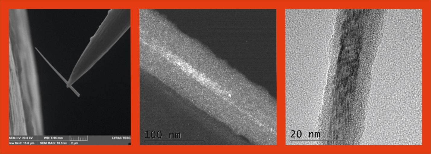
CuSix cathode for electrochemical CO2 reduction
 The CVD deposition method was used to prepare a copper silicide cathode CuxSi (3<x<5). Butylsilane BuSiH3 was passed in a quartz tube over a Cu substrate, thermally decomposed at 550 °C and 300-400 Pa pressure, forming a porous copper silicide structure and nanostructures with predominantly nano- and micro-rods on the surface. Two different versions of the catalyst grew at different precursor flow rates - one had a SiCx layer grown on it, while the other did not. Both variants retained catalytic activity without significant reduction even after 720 h of electrochemical measurements. The CuxSi catalyst showed high selectivity towards ethanol (~79%) in neutral CO2-saturated electrolyte and acetic acid (~72%) in alkaline medium.
- Dřínek V., Dytrych P., Fajgar R., Klementová M., Kupčík J., Kopeček J., Svora P., Koštejn M., Jandová V., Soukup K., Beranek R.: A robust and high performance copper silicide catalyst for electrochemical CO2 reduction. Materials Advances, 2024. DOI
CrGex nanowires synthesis
 Using the CVD technique, nanowires were prepared from GeH4 and Cr(acac)3 precursors. Cr(acac)3 precursor was vaporized at 110 °C and transferred in GeH4 stream to an oven-hot zone at 550 °C where pyrolysis took place. The synthesized nanowires are composed of a crystalline Ge core and an amorphous jacket from a CrGex alloy with composition [Cr]:[Ge]=1:(6-7). The electrical resistance of a system nanowire-substrate is 2,7 kW.cm which results probably from the presence of deep centres in the Ge gap generated by Cr atoms. Besides nanowires, Ge nanoballs were grown in deposits during the CVD process. Probably, the nanoballs served as initiation centers for CrGex nanowire growth.
- Dřínek V., Tiagulskyi S., Yatskiv R., Grym J., Fajgar R., Jandová V., Koštejn M., Kupčík J., Chemical vapor deposition of germanium-rich CrGex nanowires. Beilstein J. Nanotechnol. 12, 1365–1371, 2023. DOI
Preparation of thin layers of ferromagnetic manganese silicides and germanides
")
 after heat treatment with Mn5Ge3 nanoparticles with diameter 10-20 nm.")
 Laser ablation of an Mn target in several Pa of a reactive background gas (SiH4 or GeH4) leads to the preparation of manganese silicides and germanides. Deposited layers are mainly amorphous; however, annealing at 600 °C (silicides) or 350 °C (germanides) triggers the crystallization of nanoparticles. Different crystalline phases of silicides (Mn4Si7, Mn5Si3, Mn5Si2) or germanides (GeMn a Mn5Ge3) can be produced, depending on the conditions (especially the pressure of a gas precursor and annealing temperature). Improvement of ferromagnetic properties is observed with increased crystallization of the layers.
Preparation of new nanostructured Yb/Si alloys
 SEM image of nanowires used for EDX elemental mapping of (b) silicon and (c) ytterbium. (d) SEM image of the deposit composed of nanowires (1000 °C) with nanowire diameter distribution.") Pulsed laser ablation of a divided Si/Yb target in an oven at temperatures between 800 and 1000 °C was performed for the preparation of nanostructures of ytterbium silicide. The nanostructured deposit was formed by nanowires, nanocolumns, and nanoparticles. The nanoparticles prepared at 800 °C were made of Yb3Si5 alloy, while nanocolumns were face-centered cubic structures together with a monoclinic phase, so far unknown for Yb/Si alloy. At 1000 °C, the prepared nanowires and nanocolumns are amorphous and decorated with nanocrystals with face-centered cubic-structured material. Nanowires prepared at 1000 °C are semiconductive at room temperature with a conductivity of 132.9 W.cm, comparable to highly doped silicon. Characterization of new structures is ongoing at ICPF and other institutes of CAS.
Pulsed laser ablation of a divided Si/Yb target in an oven at temperatures between 800 and 1000 °C was performed for the preparation of nanostructures of ytterbium silicide. The nanostructured deposit was formed by nanowires, nanocolumns, and nanoparticles. The nanoparticles prepared at 800 °C were made of Yb3Si5 alloy, while nanocolumns were face-centered cubic structures together with a monoclinic phase, so far unknown for Yb/Si alloy. At 1000 °C, the prepared nanowires and nanocolumns are amorphous and decorated with nanocrystals with face-centered cubic-structured material. Nanowires prepared at 1000 °C are semiconductive at room temperature with a conductivity of 132.9 W.cm, comparable to highly doped silicon. Characterization of new structures is ongoing at ICPF and other institutes of CAS.